Views: 0 Author: Site Editor Publish Time: 2026-03-24 Origin: Site


In photovoltaic modules, there is an unremarkable yet crucial component - the photovoltaic junction box. It undertakes the dual mission of current transmission and module protection, and is an indispensable "unsung hero" in the photovoltaic system. In this small box, power semiconductor devices are staging a technological drama concerning efficiency and safety.
Junction box: The dual mission of connection and protection
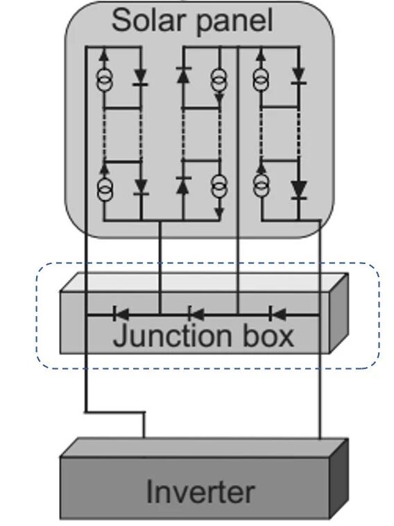
The role of junction boxes in solar cell modules can be summarized into two points: connection and transmission as well as module protection. Solar cell modules perform photoelectric conversion through solar cells, and the generated electricity must be transmitted to the charging and control systems through junction boxes. Meanwhile, the junction box also serves as the "link" of the entire solar array, connecting numerous components together to form the power generation whole.
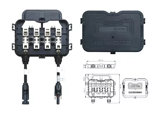
But the junction box has a more important mission - to protect the components. When the components in the formation are blocked by dark clouds, tree branches, bird droppings, etc., a "hot spot effect" will form in some local areas, which not only affects power generation but may even damage the components in severe cases. At this point, the protection mechanism inside the junction box will be activated, bypassing the faulty battery string to protect the entire component and even the array.
Considering cost and process, the current industry generally adopts the solution of configuring a protection device on a series of battery strings, which is both simple and effective.
Power semiconductor: The core component of bypass units
Among the protective functions of the junction box, the power semiconductor device inside it - the bypass diode - truly plays a core role. It takes advantage of the unidirectional conductivity of semiconductor materials. During normal operation, it consumes almost no electrical energy, but when the components are blocked, it quickly conducts, providing a detour channel for the current.
From a technical perspective, bypass diodes need to meet harsh working conditions: a wide temperature range in outdoor environments, long-term stable electrical performance, and the ability to handle unexpected situations. Especially when photovoltaic modules are blocked, diodes need to withstand large current impacts within a short period of time while effectively dissipating the generated heat.
This is precisely where Schottky diodes demonstrate their advantages. Schottky diodes feature a low forward voltage drop and fast switching speed, which can effectively reduce power loss during normal operation and respond quickly when protection is needed.
In practical applications, the performance of diodes directly affects the protection effect of junction boxes. Forward voltage drop determines the energy loss of a diode during operation, leakage current affects the safety of the system, and thermal performance is related to the reliability of long-term operation.
Reliability verification of photovoltaic junction boxes
As a component that operates outdoors for a long time, the reliability of the junction box is of vital importance. Industry standards have strict verification requirements for the performance of bypass diodes to ensure reliable operation under various harsh conditions.
In a typical reliability test, components are placed in a high-temperature environment while being passed through a current that simulates the actual working conditions. After a certain period of continuous current flow, it is necessary to test the working state of the diode to verify whether it can remain stable under the dual tests of high temperature and large current. Furthermore, the test conditions will be even more stringent to simulate the working conditions under extreme circumstances.

These verifications are not only a test of the overall design of the junction box, but also a strict screening of the power semiconductor devices inside it. Only those diodes that meet the requirements in terms of design, materials and craftsmanship can perform well in such tests, ensuring a service life of up to 25 years for photovoltaic modules.
Industry trend: From passive protection to intelligent interconnection
As the photovoltaic industry moves towards high efficiency and high reliability, the junction box itself is also undergoing technological upgrades. On the one hand, the continuous increase in component power has put forward higher requirements for the current-carrying capacity of junction boxes. Thicker cables and connection technologies with lower resistance have become the development trend. On the other hand, the rise of emerging application scenarios such as offshore photovoltaic has driven junction boxes to evolve towards higher waterproof levels and stronger weather resistance.
The material revolution of power devices
At the level of power semiconductors, technological progress is also advancing at an unprecedented pace. The traditional Schottky diode has been continuously optimized, with its forward voltage drop constantly decreasing and its heat dissipation performance continuously improving, adapting to the current increase requirements brought by large-sized silicon wafers. Meanwhile, wide bandgap semiconductor materials represented by silicon carbide began to enter the field of photovoltaic junction boxes. Silicon carbide devices have higher withstand voltage capacity, better high-temperature characteristics and lower switching losses. Although their large-scale application in the field of bypass diodes still requires time, their technical potential has already attracted industry attention.
The future trend of intelligent interconnection
Intelligence is also a direction that cannot be ignored. The new generation of "intelligent junction box", on the basis of traditional protection functions, has added monitoring and control capabilities. It can monitor the working status of each battery string in real time, conduct refined management, and provide data support for system operation and maintenance. From simple protection to a balance between protection and intelligence, junction boxes are undergoing a transformation from "passive protection" to "active management". This transformation is not only supported by power semiconductors but also inseparable from the coordinated development of technologies such as control chips and communication modules.

From simple connection transmission to intelligent component management, the technological evolution of junction boxes has never ceased. In this small box, power semiconductor devices have always played a core role.
Sanders products empower photovoltaic junction boxes
Sanders Microelectronics (SMC) was founded in 1997 and is a Sino-US joint venture high-tech enterprise integrating semiconductor research and development, design, manufacturing and sales. Our semiconductor chips, power semiconductor devices and other products are widely used in various fields such as communication, consumer goods, industry, renewable energy, electric vehicles, etc., and at the same time meet the high reliability requirements of cutting-edge industries such as avionics and medical devices.
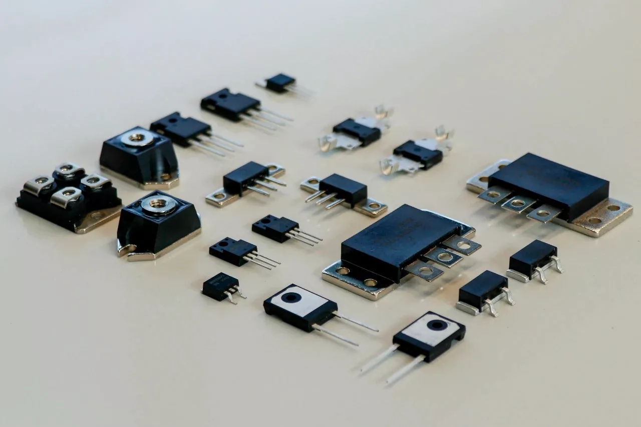
As a globally leading manufacturer of power semiconductors, SMC Sanders has nearly 30 years of technological accumulation and is highly trusted by customers. Our high-performance silicon carbide MOSFET, silicon carbide diodes, ultra-fast recovery diodes, silicon-based power diodes and other products feature high efficiency, high reliability and good cost performance, which can provide strong support for the application of photovoltaic junction boxes and system upgrades. Sanders' professional service teams all over the world offer you the ultimate customer service experience and safeguard your product design.
Some products of SMC Sanders that can be applied to photovoltaic junction boxes are as follows.